Defining the energy properties of CdI2 film by experimental and theoretical methods
DOI:
https://doi.org/10.15587/1729-4061.2025.341823Keywords:
band gap, Urbach energy, absorption spectra, density functional theoryAbstract
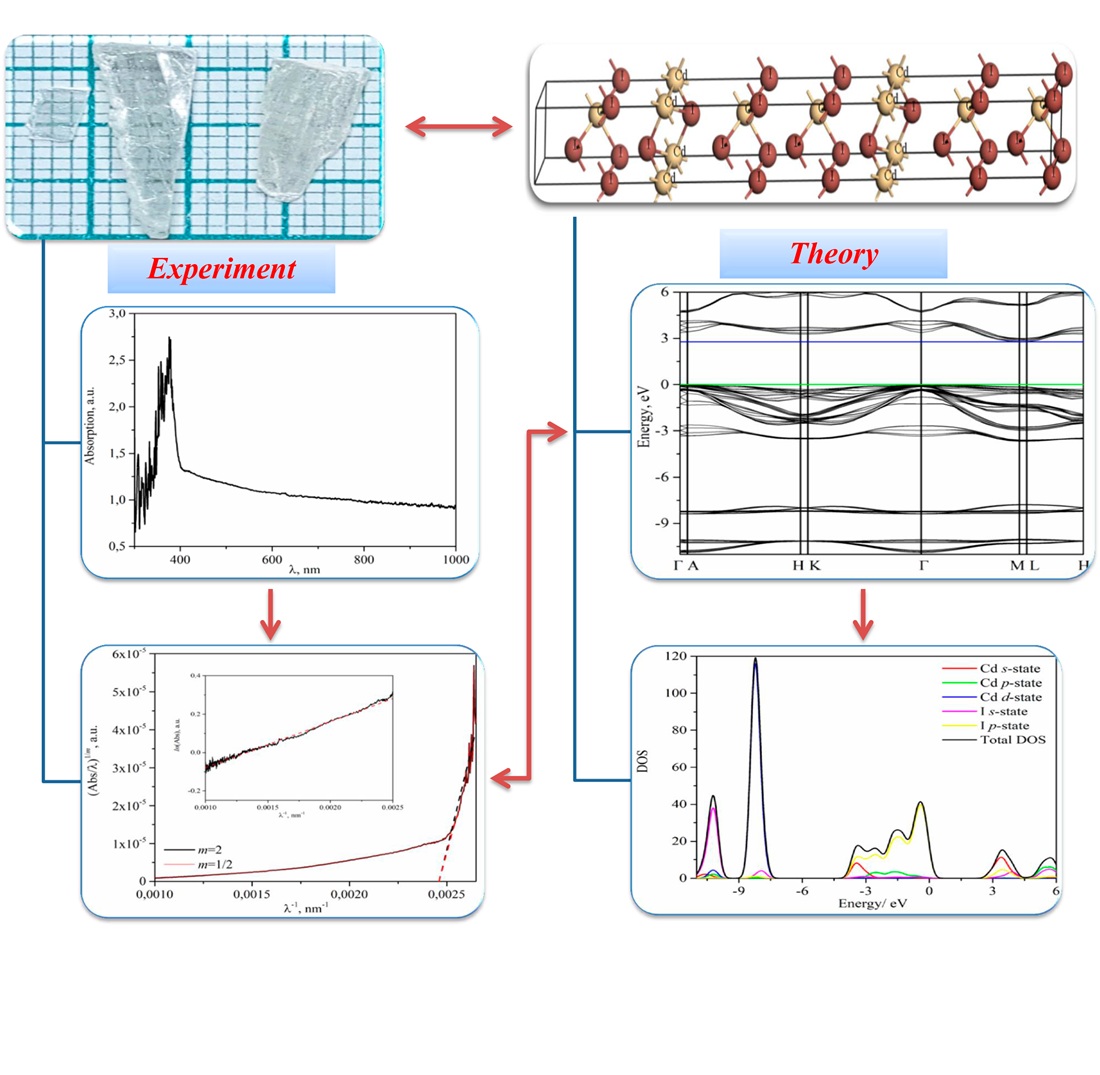
This study investigates the compound CdI2, which is actively used as a component in scintillation detectors for the detection of alpha-particle radiation. The research addresses the task to correlate experimental results with theoretically determined parameters of CdI2 films. One of the primary objectives for studying this compound is to determine its electronic structure and optical properties.
The CdI2 thick film was obtained by cleaving from a bulk sample. The average thickness of the CdI2 thick film is 2 μm. The optical properties of CdI2 thick film were investigated by optical absorption spectra. The absorption spectrum fitting method was applied to estimate the optical band gap and Urbach energy of the CdI2 thick film. This method requires only the measurement of the absorbance spectrum, and no additional information, such as the film thickness or reflectance spectra. The optical band gaps and Urbach energy obtained for the CdI2 thick film are 3.05 eV and 5.17 eV, respectively.
Electronic band structure and energy properties were studied for CdI2. We calculated the electron dispersion at high symmetry directions of the Brillouin zone and density of electron estimated with the generalized gradient approximation (GGA). A Perdew–Burke–Ernzerhof functional for solids (PBEsol) was applied. Based on the dispersion of energy bands, the predominant type of conductivity in the studied materials was determined.
Consistency of theoretical and experimental parameters exceeds that reported in previous studies, which supports the use of CdI2 as a model compound, especially in the search and design of novel crystalline materials. The established parameters could be used in the development of components for a scintillation detector
References
- Lavrentyev, A. A., Gabrelian, B. V., Vu, T. V., Ananchenko, L. N., Myronchuk, G. L., Parasyuk, O. V. et al. (2019). Electronic and optical properties of quaternary sulfide Tl2HgSnS4, a promising optoelectronic semiconductor: A combined experimental and theoretical study. Optical Materials, 92, 294–302. https://doi.org/10.1016/j.optmat.2019.04.032
- Rudysh, M. Y., Pryshko, I. A., Shchepanskyi, P. A., Stadnyk, V. Y., Brezvin, R. S., Kogut, Z. O. (2022). Optical and electronic parameters of Rb2SO4 crystals. Optik, 269, 169875. https://doi.org/10.1016/j.ijleo.2022.169875
- Vu, T. V., Luzhnyi, I. V., Myronchuk, G. L., Bekenev, V. L., Bohdanyuk, M. S., Lavrentyev, A. A. et al. (2021). DFT calculations and experimental studies of the electronic structure and optical properties of Tl4PbI6. Optical Materials, 114, 110982. https://doi.org/10.1016/j.optmat.2021.110982
- Rudysh, M. Ya. (2022). Electronic structure, optical and elastic properties of AgAlS2 crystal under hydrostatic pressure. Materials Science in Semiconductor Processing, 148, 106814. https://doi.org/10.1016/j.mssp.2022.106814
- Ai, R., Guan, X., Li, J., Yao, K., Chen, P., Zhang, Z., Duan, X., Duan, X. (2017). Growth of Single-Crystalline Cadmium Iodide Nanoplates, CdI2/MoS2 (WS2, WSe2) van der Waals Heterostructures, and Patterned Arrays. ACS Nano, 11 (3), 3413–3419. https://doi.org/10.1021/acsnano.7b01507
- Qasrawi, A. F., Hamarsheh, A. A. (2021). Au/CdBr2/SiO2/Au Straddling‐Type Heterojunctions Designed as Microwave Multiband Pass Filters, Negative Capacitance Transistors, and Current Rectifiers. Physica Status Solidi (a), 218 (22). https://doi.org/10.1002/pssa.202100327
- Popov, G., Mattinen, M., Hatanpää, T., Vehkamäki, M., Kemell, M., Mizohata, K. et al. (2019). Atomic Layer Deposition of PbI2 Thin Films. Chemistry of Materials, 31 (3), 1101–1109. https://doi.org/10.1021/acs.chemmater.8b04969
- Kashuba, A., Zhydachevskyy, Y., Semkiv, I., Franiv, A., Kushnir, O. (2018). Photoluminescence in the solid solution In0.5Tl0.5I. Ukrainian Journal of Physical Optics, 19 (1), 1. https://doi.org/10.3116/16091833/19/1/1/2018
- Rybak, O. V. (2024). Thermodynamic Analysis of the Equilibrium Vapor Phase Composition of the Cd-I2 System. Journal of Nano- and Electronic Physics, 16 (1), 01021-1-01021–01024. https://doi.org/10.21272/jnep.16(1).01021
- Kaur, H. (2014). Growth and formation of polytypes in crystals of cadmium iodide. Applied Science Research, 6 (1), 64–66. Available at: https://www.scholarsresearchlibrary.com/articles/growth-and-formation-of-polytypes-in-crystals-of-cadmium-iodide.pdf
- Bai, X., Jiang, Q., Song, P., Jia, Z.-P., Lu, S., Gao, Z.-K. et al. (2023). Study of electronic and optical properties of CdI2 modulated by electric field: a first-principles study. Optics Express, 31 (19), 31504. https://doi.org/10.1364/oe.497833
- Momin, Md. A., Islam, Md. A., Nesa, M., Sharmin, M., Rahman, M. J., Bhuiyan, A. H. (2021). Effect of M (Ni, Cu, Zn) doping on the structural, electronic, optical, and thermal properties of CdI2: DFT based theoretical studies. AIP Advances, 11 (5). https://doi.org/10.1063/5.0050145
- Tao, L., Huang, L. (2017). Computational design of enhanced photocatalytic activity of two-dimensional cadmium iodide. RSC Advances, 7 (84), 53653–53657. https://doi.org/10.1039/c7ra09687a
- Tyagi, P., Vedeshwar, A. G. (2002). Grain size dependent optical properties of CdI2films. The European Physical Journal Applied Physics, 19 (1), 3–13. https://doi.org/10.1051/epjap:2002043
- Kariper, İ. A. (2016). Structural, optical and porosity properties of CdI2 thin film. Journal of Materials Research and Technology, 5 (1), 77–83. https://doi.org/10.1016/j.jmrt.2015.10.005
- Tyagi, P., Vedeshwar, A. G., Mehra, N. C. (2001). Thickness dependent optical properties of CdI2 films. Physica B: Condensed Matter, 304 (1-4), 166–174. https://doi.org/10.1016/s0921-4526(01)00392-1
- Yan, Z., Yin, K., Yu, Z., Li, X., Li, M., Yuan, Y. et al. (2020). Pressure-induced band-gap closure and metallization in two-dimensional transition metal halide CdI2. Applied Materials Today, 18, 100532. https://doi.org/10.1016/j.apmt.2019.100532
- Kunyo, I. M., Kashuba, A. I., Karpa, I. V., Stakhura, V. B., Sveleba, S. A., Katerynchuk, I. M. et al. (2018). The band energy structure of (N(CH3)4)2ZnCl4 crystals. Journal of Physical Studies, 22 (3). https://doi.org/10.30970/jps.22.3301
- Perdew, J. P., Ruzsinszky, A., Csonka, G. I., Vydrov, O. A., Scuseria, G. E., Constantin, L. A. et al. (2008). Restoring the Density-Gradient Expansion for Exchange in Solids and Surfaces. Physical Review Letters, 100 (13). https://doi.org/10.1103/physrevlett.100.136406
- Ilchuk, H., Semkiv, I., Huminilovych, R., Yuryev, S., Rudysh, M., Kashuba, A. (2025). Effect of deposition time on the absorption spectra of CdS nanostructured films. Journal of Physical Studies, 29 (3). https://doi.org/10.30970/jps.29.3702
- Ghobadi, N. (2013). Band gap determination using absorption spectrum fitting procedure. International Nano Letters, 3 (1). https://doi.org/10.1186/2228-5326-3-2
- Kashuba, A. I. (2023). Influence of metal atom substitution on the electronic and optical properties of solid-state Cd0.75X0.25Te (X= Cu, Ag and Au) solutions. Physics and Chemistry of Solid State, 24 (1), 92–101. https://doi.org/10.15330/pcss.24.1.92-101
Downloads
Published
How to Cite
Issue
Section
License
Copyright (c) 2025 Mykola Solovyov, Ihor Semkiv, Andrii Kashuba

This work is licensed under a Creative Commons Attribution 4.0 International License.
The consolidation and conditions for the transfer of copyright (identification of authorship) is carried out in the License Agreement. In particular, the authors reserve the right to the authorship of their manuscript and transfer the first publication of this work to the journal under the terms of the Creative Commons CC BY license. At the same time, they have the right to conclude on their own additional agreements concerning the non-exclusive distribution of the work in the form in which it was published by this journal, but provided that the link to the first publication of the article in this journal is preserved.
A license agreement is a document in which the author warrants that he/she owns all copyright for the work (manuscript, article, etc.).
The authors, signing the License Agreement with TECHNOLOGY CENTER PC, have all rights to the further use of their work, provided that they link to our edition in which the work was published.
According to the terms of the License Agreement, the Publisher TECHNOLOGY CENTER PC does not take away your copyrights and receives permission from the authors to use and dissemination of the publication through the world's scientific resources (own electronic resources, scientometric databases, repositories, libraries, etc.).
In the absence of a signed License Agreement or in the absence of this agreement of identifiers allowing to identify the identity of the author, the editors have no right to work with the manuscript.
It is important to remember that there is another type of agreement between authors and publishers – when copyright is transferred from the authors to the publisher. In this case, the authors lose ownership of their work and may not use it in any way.